
ASML Begins India Operations, Partners with Tata Electronics for 300 mm Semiconductor Fab in Gujarat
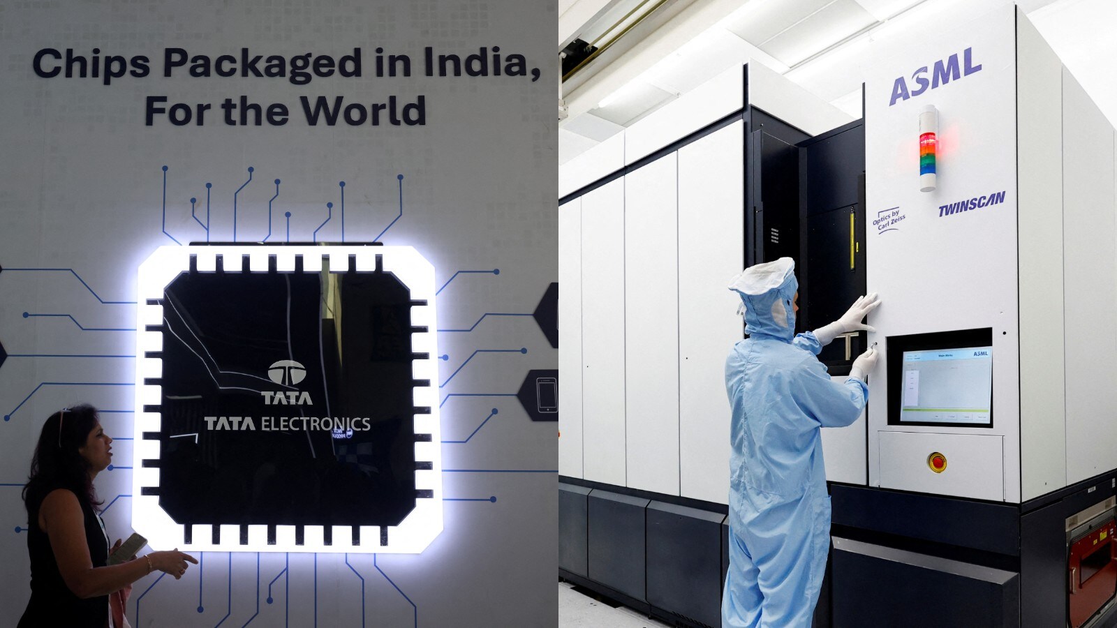
In September 2026, ASML, a Dutch leader in semiconductor lithography systems, commenced its operations in India and established a legal entity. ASML partnered with Tata Electronics to support the establishment and ramp-up of India's first commercial 300 mm semiconductor fabrication facility in Dholera, Gujarat, involving an $11 billion investment. The fab aims to produce 50,000 wafers monthly targeting automotive, mobile devices, and AI applications, with operations expected to start by 2028. This development aligns with India's Semicon 2.0 scheme, which fosters semiconductor ecosystem growth through incentives totaling approximately ₹1.27 lakh crore (~$13.5 billion). India targets meeting 15-25% of its semiconductor demand locally by 2032, requiring multiple fabrication plants and ecosystem support.
On this page
Key Facts
- ASML began its India operations in September 2026, setting up a customer support office and planning to hire 20-30 young engineering graduates.
- Tata Electronics and ASML signed a strategic Memorandum of Understanding (MoU) in May 2026 to deploy ASML's advanced lithography tools and solutions at Tata Electronics’ 300 mm semiconductor fabrication plant in Dholera, Gujarat.
- The Dholera fab, with an investment of approximately $11 billion, is designed to produce 50,000 wafers per month using technology nodes ranging from 28nm to 110nm, targeting markets including automotive, mobile devices, and artificial intelligence.
- India’s Semicon 2.0 scheme offers incentives of about ₹1.27 lakh crore (approximately $13.5 billion) to boost semiconductor manufacturing and ecosystem development.
- India aims to fulfill 15 to 25 percent of its local semiconductor demand by 2032, necessitating the establishment of multiple fabrication plants and supporting infrastructure.
Background & Context
ASML, headquartered in the Netherlands, is the world’s leading supplier of photolithography equipment essential for semiconductor fabrication. Lithography systems transfer intricate circuit patterns onto silicon wafers, a critical process in chip manufacturing. The industry standard wafer size for advanced fabs is 300 mm (12 inches), and Tata Electronics is developing India’s first commercial 300 mm semiconductor fab in Dholera, a planned industrial city in Gujarat. The partnership with ASML ensures access to advanced lithography technology, vital for the fab’s successful ramp-up and high-quality production.
This collaboration is a key milestone in India’s broader aim to establish a self-reliant semiconductor ecosystem, reducing dependence on imports and advancing domestic manufacturing capabilities under the Semicon 2.0 initiative. The initiative’s incentives encourage investments across fabrication, supply chain development, and research, enhancing India’s position in the global semiconductor industry.
Why This Matters for Exams
The establishment of ASML’s operations in India and its strategic partnership with Tata Electronics is a landmark development highlighting India’s expanding semiconductor ambitions. It is relevant for current affairs sections on technology advancement, industrial policy, and international collaborations. Awareness of Semicon 2.0 and large-scale investments such as the Tata Electronics fab in Gujarat is important for understanding India’s strategy to become a significant semiconductor manufacturer and technology hub.
Points to Remember
- ASML is a Dutch technology company renowned for lithography systems crucial in semiconductor manufacturing.
- Tata Electronics is building India’s first commercial 300 mm wafer semiconductor fab at Dholera, Gujarat.
- The fab involves an investment of $11 billion, with plans to produce 50,000 wafers per month at technology nodes from 28nm to 110nm.
- The Semicon 2.0 scheme provides approximately ₹1.27 lakh crore (~$13.5 billion) in incentives to promote semiconductor manufacturing and ecosystem development in India.
- India targets fulfilling 15-25% of its semiconductor demand locally by 2032, requiring multiple fabrication facilities.
- Dholera is a planned industrial hub in Gujarat, chosen as the site for the semiconductor fabrication plant.
Practice MCQs
Question 1
- Which company began semiconductor-related operations in India in September 2026?
- Samsung
- ASML
- TSMC
- Intel
Answer: C. ASML
Question 2
- Where is India’s first commercial 300 mm semiconductor fabrication plant being established?
- Bengaluru
- Dholera, Gujarat
- Hyderabad
- Noida
Answer: B. Dholera, Gujarat
Question 3
- What is the approximate investment planned for Tata Electronics’ 300 mm semiconductor fab?
- $1 billion
- $5 billion
- $11 billion
- $25 billion
Answer: C. $11 billion
Sources & Further Reading
| Document / Website | Link |
|---|---|
| ASML Begins India Operations – GKToday | Open ASML Begins India Operations – GKToday ↗www.gktoday.in |
| Tata Electronics and ASML Announce Strategic Partnership to Advance the Semiconductor Manufacturing Ecosystem in India | Open Tata Electronics and ASML Announce Strategic Partnership to Advance the Semiconductor Manufacturing Ecosystem in India ↗www.asml.com |
| India Semiconductor Mission 2.0 | Open India Semiconductor Mission 2.0 ↗static.pib.gov.in |
| Semiconductor Foundry - Tata Electronics - Tata Electronics - Tata Electronics Private Limited | Open Semiconductor Foundry - Tata Electronics - Tata Electronics - Tata Electronics Private Limited ↗tataelectronics.com |