
Odisha Signs MoU with Intel and 3D Glass Solutions for India’s First Advanced 3D Semiconductor Packaging Unit
On 28-29 May 2026, Odisha signed a Memorandum of Understanding (MoU) with Intel and 3D Glass Solutions (3DGS) to establish India’s first advanced 3D glass semiconductor substrate manufacturing and chip packaging facility at Info Valley, Bhubaneswar. With a total investment of approximately Rs 1,943.53 crore under the India Semiconductor Mission, the plant will produce 70,000 glass substrates and 50 million assembled units annually, focusing on cutting-edge sectors like AI, defence electronics, and 5G. The facility is expected to start commercial production by August 2028, positioning Odisha as a key hub in India’s semiconductor ecosystem.
On this page
Key Facts
- In late May 2026 (28th and 29th May), the Government of Odisha signed a Memorandum of Understanding (MoU) with Intel and 3D Glass Solutions (3DGS) to bring advanced semiconductor substrate manufacturing technology to India.
- The project is located at Info Valley, Bhubaneswar, Khordha district, Odisha.
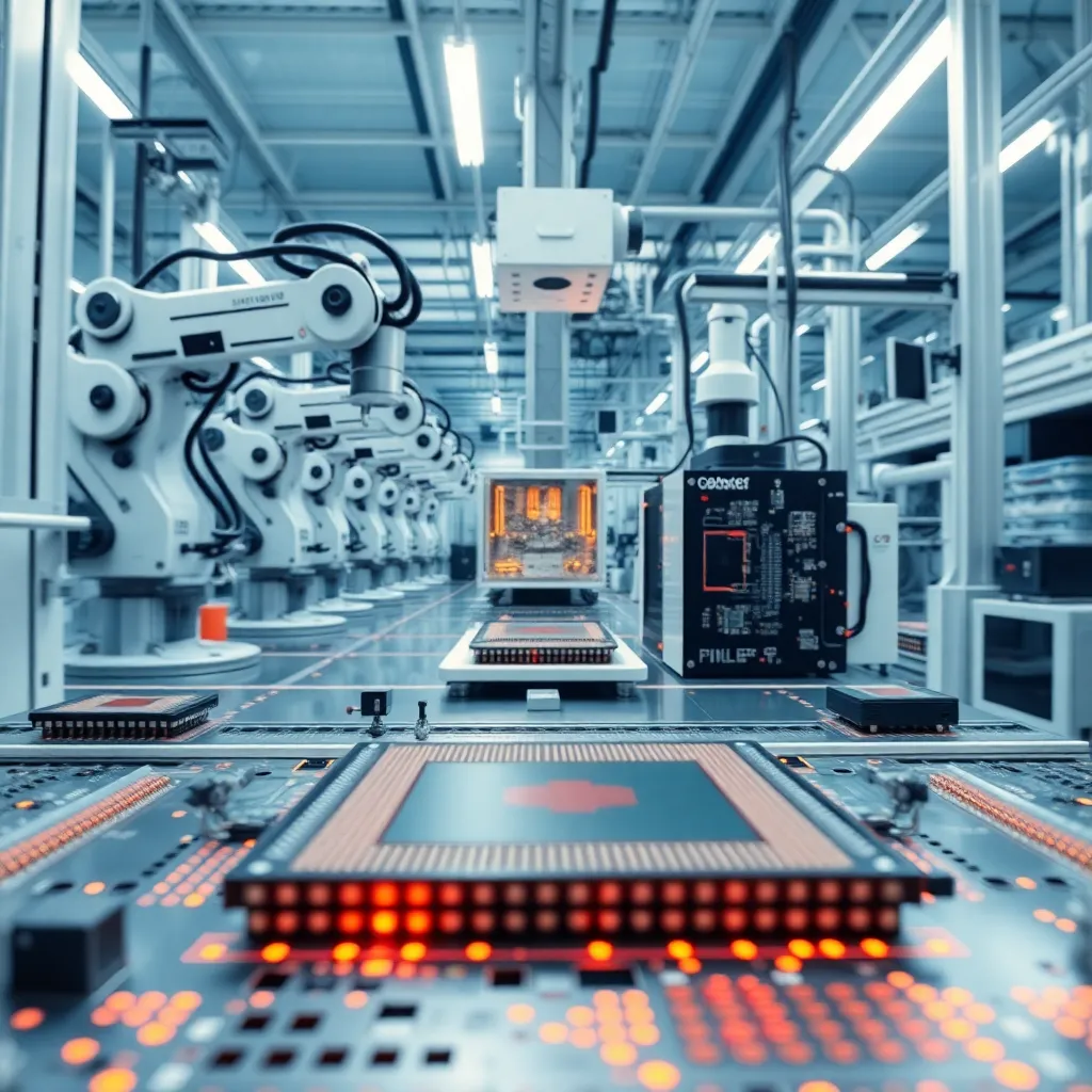
- The initiative focuses on coating, packaging, and producing glass substrates and advanced 3D heterogeneous integration modules for semiconductor chips.
- The total project cost is estimated at approximately Rs 1,943.53 crore, with the Central Government providing Rs 799 crore and the Odisha State Government contributing roughly Rs 399.5 crore.
- This project was formally approved under the India Semiconductor Mission (ISM) in August 2025.
- The manufacturing facility is promoted and implemented by the US-based company 3D Glass Solutions Inc. through its wholly owned Indian subsidiary, Heterogeneous Integration Packaging Solutions Private Limited.
- Expected annual production capacities include about 70,000 glass substrates, 50 million assembled units, and nearly 13,000 advanced 3D heterogeneous integration modules.
- Commercial production is anticipated to commence by August 2028.
- 3D heterogeneous integration involves packaging multiple different chip types (like processors, memory, sensors) in a single compact module, supporting advanced applications.
Background & Context
Semiconductor packaging is an essential step where integrated circuits are enclosed and interconnected to form a functional chip ready for use in electronics. The project emphasises the use of glass substrates, which enable high-density interconnections and support advanced 3D stacking and heterogeneous integration technologies, critical for modern applications such as artificial intelligence (AI), high-performance computing, defence electronics, and next-generation telecommunications including 5G.
Odisha, historically known for its mineral resources and energy sector, is rapidly evolving into a semiconductor and electronics manufacturing hub. The India Semiconductor Mission, a central government initiative, aims to boost domestic semiconductor production capabilities, reducing reliance on imports and furthering the 'Atmanirbhar Bharat' vision of self-reliance.
Besides the 3D Glass packaging unit, Odisha is also set to host India's first commercial compound semiconductor fabrication unit, developed by Chennai-based SiCSem in partnership with UK-based Clas-SiC Wafer Fab, with groundbreaking scheduled for June 2026. Compound semiconductors, made from materials like silicon carbide and gallium nitride, are vital for high-power and high-frequency applications such as electric vehicles (EVs), renewable energy, and telecommunications.
Why This Matters for Exams / Exam Relevance
- Represents a significant milestone in India’s semiconductor manufacturing ecosystem, essential for questions on industrial development, technology advancements, and government initiatives in science & technology.
- Mention of key stakeholders: Odisha government, Intel, 3D Glass Solutions, and their collaboration reflects international partnerships fostering India’s technological growth.
- Important dates (agreement in May 2026, approval in August 2025, production by August 2028) are potential factual points for current affairs sections.
- The project ties directly to India's strategic goals like the India Semiconductor Mission and Atmanirbhar Bharat, frequently examined themes.
- Technologies such as advanced 3D heterogeneous integration and compound semiconductors are emerging topics under science and technology syllabus.
- Geographically, Odisha's emergence as a semiconductor hub links to economic geography and developmental studies.
Points to Remember
- Location: Info Valley, Bhubaneswar, Odisha, is the site of India’s first advanced 3D glass semiconductor packaging facility.
- The MoU signed in May 2026 is a partnership between Odisha government, Intel, and 3D Glass Solutions Inc., implemented via its Indian subsidiary.
- The project is funded under the India Semiconductor Mission approved in August 2025 with a total investment of nearly Rs 1,943.53 crore.
- Expected commercial production start date is August 2028.
- Focus sectors served include Artificial Intelligence, high-performance computing, defence electronics, and next-generation telecom systems.
- Odisha simultaneously progresses with India’s first commercial compound semiconductor fabrication plant by SiCSem and Clas-SiC, groundbreaking planned June 2026.
- Compound semiconductors like silicon carbide enable critical high-power applications such as EVs, renewable energy, and communications.
Sources & Further Reading
| Document / Website | Link |
|---|---|
| Odisha Signs Semiconductor MoU with Intel and 3DGS | Open Odisha Signs Semiconductor MoU with Intel and 3DGS ↗www.gktoday.in |
| Groundbreaking of India’s First Advanced 3D Semiconductor Packaging Unit in Odisha; Major Boost to AI, 5G and Defence Tech | Open Groundbreaking of India’s First Advanced 3D Semiconductor Packaging Unit in Odisha; Major Boost to AI, 5G and Defence Tech ↗www.pib.gov.in |
| Odisha govt signs semiconductor substrate manufacturing pact with Intel, 3DGS: Ashwini Vaishnaw | Open Odisha govt signs semiconductor substrate manufacturing pact with Intel, 3DGS: Ashwini Vaishnaw ↗ianslive.in |
| SiCSem breaks ground on India's first SiC fab - Compound Semiconductor News | Open SiCSem breaks ground on India's first SiC fab - Compound Semiconductor News ↗compoundsemiconductor.net |
| India's 1st advanced 3D glass chip packaging unit to come up in Bhubaneswar | Open India's 1st advanced 3D glass chip packaging unit to come up in Bhubaneswar ↗www.business-standard.com |
| India gets first advanced 3D chip packaging plant, Intel helping it set up in Odisha | Open India gets first advanced 3D chip packaging plant, Intel helping it set up in Odisha ↗www.indiatoday.in |